 日本語
日本語 





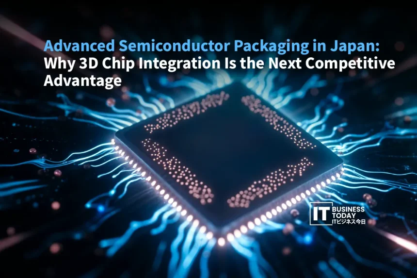
For decades, semiconductor leadership was measured by one simple metric, who could make the smallest transistor. That race is now entering a different phase. As traditional chip scaling becomes harder due to physical limits, rising costs, and growing power challenges, the next competitive battlefield is moving toward how efficiently multiple chips can work together inside a single package.
This is where advanced semiconductor packaging starts turning into a real strategic advantage. Japan has that solid base in materials science, very precise manufacturing, and semiconductor equipment so it’s now leaning toward 3D chip integration, not just chasing transistor scaling like everyone else. You can see it in stuff like chiplets, hybrid bonding, high bandwidth memory, automotive semiconductors, and Edge AI that are really starting to pick up speed. Japan is basically shaping an ecosystem meant for the next wave of computing.
In fact, METI’s 2026 New Year message pointed this out pretty directly, saying Japan intends to invest 100 billion yen in Rapidus, going forward. It fits into a wider plan where advanced packaging becomes one of the main pillars in Japan’s semiconductor comeback, not just an accessory.

Also Read: AI Cloud Cost Optimization: Strategies for Balancing Performance, Cost, and Sustainability in Enterprise IT
The Strategic Pivot to Advanced 3D Packaging
The semiconductor industry has spent decades following Moore’s Law, where smaller transistors delivered higher performance and lower costs. However, that approach is becoming increasingly difficult. Manufacturing smaller nodes requires massive investments, while engineers face growing challenges around heat generation, power consumption, and data movement inside chips.
The problem is no longer only about transistor density. It is about communication between different parts of a computing system.
Traditional 2D chip designs place logic, memory, and other functions on a single flat layer. But as workloads become heavier, especially with AI and high-performance computing, moving data across these layers creates bottlenecks. The distance between processing units and memory directly affects speed and energy efficiency.
Advanced semiconductor packaging changes this equation.
Instead of building one massive chip, manufacturers are moving toward heterogeneous integration, where different chip components are combined into one advanced package. System-in-Package (SiP) and chiplet architectures allow companies to integrate specialised components such as processors, memory, and sensors vertically or side by side.
Japan is actively building capabilities in this direction. The Leading-edge Semiconductor Technology Center (LSTC) was established on December 21, 2022, and now has 18 participating institutions. The organisation is also involved in three NEDO projects, including Beyond 2nm semiconductor development, Edge AI accelerator development, and chiplet-based custom SoC design platform development.
The shift is significant because future semiconductor leadership may not depend only on who creates the smallest chip. It may depend on who can combine multiple chips into the most efficient computing system.
Materials Equipment and Precision Substrates
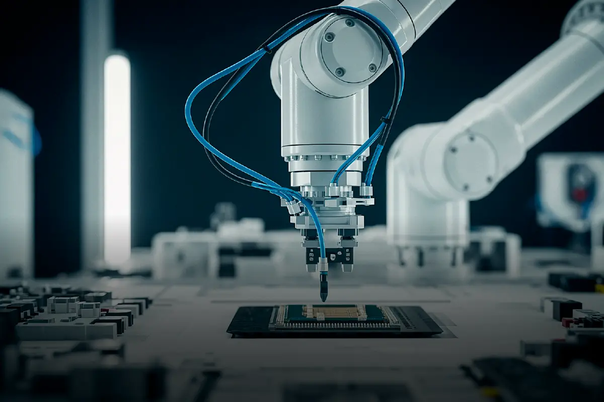
Japan’s advantage in advanced semiconductor packing doesn’t really trace back to one company or one single technology. It’s more like the whole situation, built up over decades, where know-how stacks across the semiconductor supply chain.
The country has developed solid strength in areas that are often less visible but still hugely important, including semiconductor materials, packaging substrates, chemical processing, and manufacturing equipment.
For advanced packaging you need specialized materials that can take higher temperatures, bigger electrical demands, and chip structures that keep getting more and more tangled. Japanese firms have been known for years for their skill in things like encapsulation materials, photoresists, and advanced substrates.
Companies such as Ibiden, Shinko Electric Industries, and Toppan work in segments that matter a lot for next generation semiconductor packages. The materials they supply shape reliability, signal quality, and even thermal management, especially once chips start packing more densely.
Equipment is another major strength.
Advanced semiconductor packaging depends on highly precise manufacturing tools, including wafer bonding systems, metrology equipment, and processes that improve chip alignment and reliability. Companies such as Tokyo Electron and DISCO represent Japan’s deeper role in semiconductor manufacturing infrastructure.
This ecosystem gives Japan a unique position. A semiconductor package is not created only at the final assembly stage. It depends on everything before it, from material quality to manufacturing precision.
Government support is also reinforcing this ecosystem. NEDO’s semiconductor programs support production-related development and next-generation technology initiatives, creating a bridge between research and commercial manufacturing.
The result is a semiconductor supply chain where Japan plays a critical role even beyond chip fabrication.
How 3D Stacking and Hybrid Bonding Re-Architect Computing
The real value of advanced semiconductor packaging comes from solving one of computing’s biggest problems, moving more data faster while consuming less energy.
3D integration addresses this by stacking multiple semiconductor dies vertically. Instead of spreading components across a larger surface area, manufacturers can bring memory, logic, and specialized processing units closer together.
One of the biggest developments in this area is hybrid bonding.
Traditional semiconductor packaging often relies on solder-based micro bumps to connect different dies. However, as chip density increases, these connections become a limitation. Hybrid bonding enables direct connections between semiconductor layers using extremely fine alignment, improving performance and reducing connection distance.
This approach is becoming increasingly important for AI workloads.
High-bandwidth memory (HBM) relies on vertical integration between memory layers and advanced logic chips. As AI models become more demanding, faster access to memory becomes just as important as processor capability.
Tokyo Electron explains that 3D Integration (3DI) packages multiple chips and functions into a single unit, making it a key technology for improving semiconductor performance. The company also highlights that bonding technology and TSV equipment are becoming essential for next-generation devices, particularly as HBM demand expands for AI semiconductors.
However, stacking chips creates new engineering challenges.
More layers mean more heat concentration. Mechanical stress, thermal cycling, and material expansion differences can impact reliability. This is why advanced substrates and thermal interface materials are becoming increasingly important.
Japan’s strength in precision materials gives it an advantage in solving these problems. The future of semiconductor performance will not only depend on faster transistors but also on better ways to connect, cool, and integrate them.
NEDO’s official profile, updated on April 15, 2026, lists 3,588.7 billion yen for the Post-5G Information and Communication Systems project and 2,170.6 billion yen for Programs for Specified Semiconductor Production-Related Development. These investments highlight the scale of Japan’s effort to strengthen next-generation semiconductor capabilities.
Automotive EVs Autonomous Systems and Edge AI
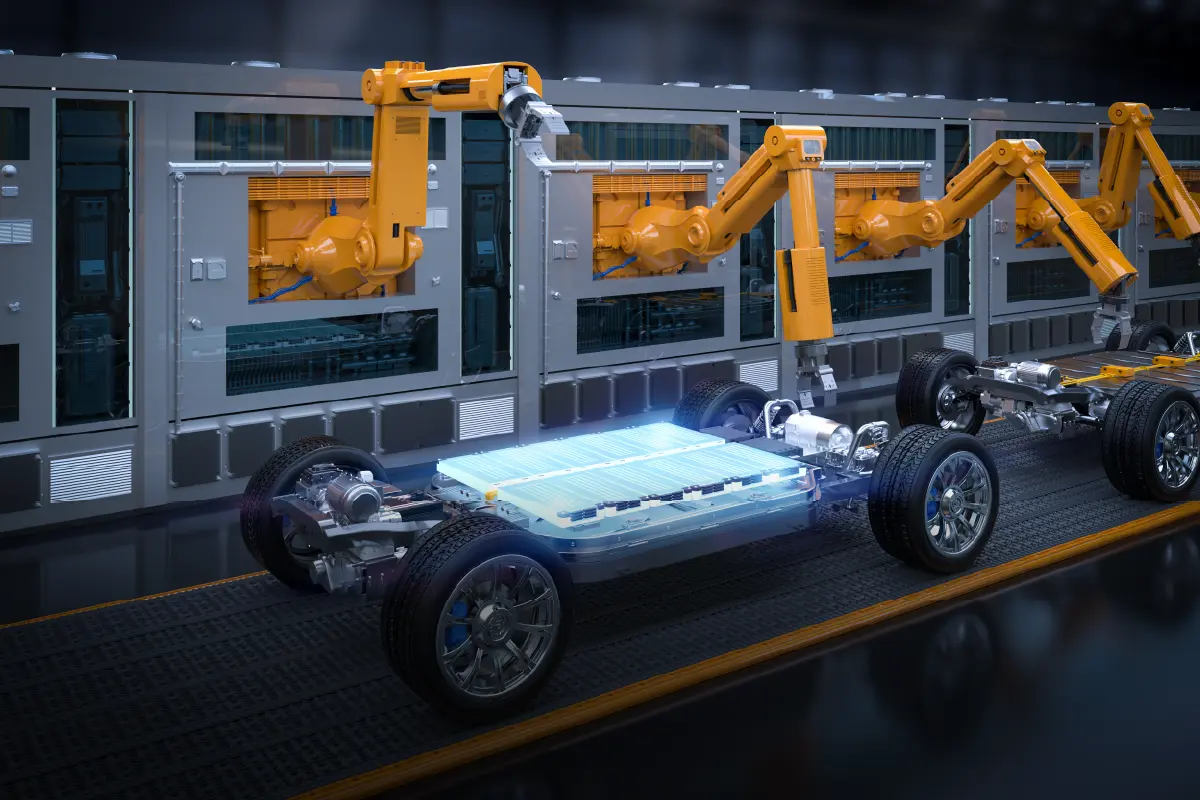
The semiconductor industry is entering a period where chips are becoming central to almost every major industrial transformation. Japan’s strongest opportunity comes from areas where it already has global expertise, particularly automotive technology.
Modern vehicles are no longer mechanical products with limited electronics. They are becoming software-defined platforms with advanced computing requirements.
Electric vehicles, autonomous driving systems, and connected vehicles also need semiconductors that can run reliably in rough settings, with heat, vibration, and those long operating cycles that never really stop.
So, naturally this is pushing demand for more advanced semiconductor packaging solutions, like not just the basic stuff.
For car use, companies can’t only chase maximum computing power. They need reliability first, plus efficiency and proper long-term durability as well. System-in-Package designs basically let manufacturers stitch together several capabilities, processing, communication, and sensing, into a smaller footprint.
Japan’s automotive ecosystem, backed by firms like Renesas and Denso, seems pretty set to gain from this shift, sooner rather than later.
Edge AI is another important driver.
As vehicles, factories, and smart devices generate more data, processing everything in the cloud creates delays and increases dependency on connectivity. Local AI processing allows systems to make faster decisions directly at the edge.
That requires compact, powerful, and efficient semiconductor designs.
Advanced semiconductor packaging enables this by bringing computing components closer together. Chiplets, high-density integration, and advanced packaging techniques can help create systems that deliver AI performance without relying only on larger chips.
Industry organisations are also recognising this shift. The JEITA JSIA platform focuses on semiconductor technology development, standardisation, intellectual property, and industry collaboration, with a dedicated Semiconductor Packaging Technical Committee.
Its 2026 policy proposal highlights that advanced packaging development will progress through areas such as optical chiplets and analog-digital mixed-integration SoC development, while targeting a semiconductor industry scale of 40 trillion yen by 2040.
The message is clear. The next wave of semiconductor growth will come from industries that need smarter, smaller, and more efficient computing systems.
The Packaging Race Will Define Semiconductor Leadership
Japan’s semiconductor comeback will not be decided only by whether it can produce cutting-edge chips. The bigger question is whether it can control the technologies that connect those chips into powerful computing systems.
Advanced semiconductor packaging gives Japan an opportunity to leverage its strongest assets, materials expertise, manufacturing precision, and equipment leadership.
For executives, the takeaway is straightforward.
| Stakeholder | Strategic Focus |
| Industry leaders | Build partnerships across materials, equipment, and chip design ecosystems |
| Engineers | Prioritise heterogeneous integration, chiplets, and thermal management |
| Supply chain teams | Track Japan’s growing role in advanced packaging infrastructure |
The semiconductor race is moving beyond smaller transistors. The winners will be those who can integrate more intelligence into less space. Japan understands that shift, and advanced 3D packaging could become its strongest path back to global semiconductor influence.



 English