 English




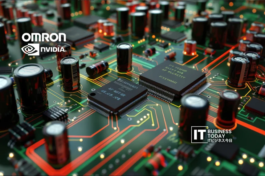
半導体のパッケージングがますます複雑化するにつれ、どういうわけか、製造工程よりも検査工程の方が、むしろ大きなボトルネックになりつつあります。課題は、単に欠陥を見つけることだけではありません。高度な技能を持つ専門家の数が減少している状況に左右されることなく、十分な早期段階で欠陥を発見することにあります。.
オムロンは、まさにその課題に取り組むため、NVIDIAとの協業を拡大しています。.
オムロンのAOIおよびAXI検査システムとNVIDIA Omniverseを組み合わせることで、同社は半導体基板の検査に向けたリアルタイムのデジタルツイン環境を構築しています。その目的は、検査精度の向上と、個々の専門知識への依存度を低減したプロセスの実現にあります。.

主な用途の一つは、製造工程における熱によって生じる部品の歪みの可視化です。こうした歪みははんだ付け不良の原因となる可能性がありますが、従来の方法では検出が難しい場合が多くあります。デジタルツイン内での物理シミュレーションを通じて、製造業者はこれらの問題を早期に特定し、不良が発生する前に熱プロファイルを調整することができます。.
こちらもお読みください: 日本におけるAIインフラの整備が加速する中、Nvidiaは冷却と電力供給の面で三菱重工業に期待を寄せています
Omron また、AOIシステムによる表面検査データと、AXI装置による内部構造データを統合することで、目に見える欠陥とその根本原因の間に潜む関連性を明らかにしています。.
また、この提携により、検査ワークフローにAIエージェントが導入されています。これを利用して NVIDIA’の動画検索・要約技術に加え、視覚言語モデルやGraph RAGを活用することで、エンジニアは自然言語で質問を行い、類似した過去の事例や検査データに基づいた説明を受け取ることができます。.
複雑さと人材不足という二つの課題に同時に直面している業界にとって、この変化は重要な意味を持ちます。.


 日本語
日本語