 日本語
日本語 





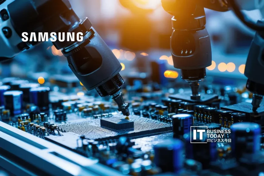
Samsung Electronics has fully opened a semiconductor research hub in Yokohama. This move strengthens its collaboration with materials suppliers, equipment makers and research organizations. The push comes as demand for chips grows with the expansion of artificial intelligence.
The Korean technology giant held an opening ceremony for the facility in Yokohama’s Minato Mirai district on September 8. 100 People attended, including Samsung executives, government representatives from Japan and South Korea and officials from Samsung’s customer companies. The research base was established in 2023. Has now reached a stage where it can conduct full-scale experiments and evaluations.
Samsung plans to invest ¥40 billion in the Japanese research base by 2028. Of that ¥20 billion will come from government subsidies. 95 Researchers from Japan and South Korea currently work at the facility.

This investment could become a development for Japan’s semiconductor ecosystem. The focus is not on chip manufacturing. Instead it centers on semiconductor packaging. This is becoming a technology for AI processors and high-performance computing.
Advanced Packaging Becomes Critical to AI Chips
As artificial intelligence workloads grow more powerful improving semiconductor performance is no longer possible by making transistors smaller alone.
Advanced packaging allows multiple semiconductor components to be combined into packages. This is especially important for AI systems that bring together processing units with high-bandwidth memory and other parts.
Samsung’s Yokohama facility is focused on back-end semiconductor technology including packaging. Samsung has described the site as a center for next-generation packaging research. Its Japanese R&D organization also lists packaging as one of its main research areas.
This creates a link with Japan’s strong presence, in semiconductor materials, manufacturing equipment and precision technologies. The collaboration could boost both innovation and supply chain resilience.
Japan’s Materials and Equipment Companies Could Benefit
A point of Samsung investment is the chance for deeper cooperation with Japanese suppliers.
Japan remains a technology provider across the semiconductor supply chain particularly in areas such as materials, wafers, manufacturing equipment and components. Samsung presence in Yokohama could give companies an opportunity to work more closely with Samsung, one of the worlds largest semiconductor manufacturers on next‑generation processes.
This could be particularly valuable to Samsung as packaging becomes more complex.
Advanced packaging needs materials, manufacturing tools, inspection tech and process‑control skills. Japanese suppliers that can help Samsung boost performance, reliability and production efficiency could find chances as AI semiconductor demand rises.
The development also fits into a recovery in Japan’s semiconductor‑related manufacturing sector. A recent Reuters survey found that sentiment among Japanese manufacturers reached its highest level since late 2021 in September driven strongly by semiconductor and data‑center demand. The electronics sectors sentiment index rose sharply to +39.
Yokohama Could Strengthen Japan’s Semiconductor R&D Network
Samsung investment also adds another research presence to Japan’s growing semiconductor ecosystem.
Japan is seeking to rebuild its position across parts of the semiconductor supply chain with government support going toward advanced manufacturing, research and related infrastructure. International companies such as TSMC have already established manufacturing operations in Japan while domestic initiatives such as Rapidus are targeting advanced semiconductor production.
Samsung’s approach is somewhat different. Than establishing the Yokohama facility primarily as a high‑volume manufacturing site Samsung is using Japan as a research and technology‑development base.
That model could be valuable for Japan because Samsung brings semiconductor expertise closer, to Japanese universities, research institutions and suppliers.
Samsung itself says its Device Solutions R&D Japan operations conduct research in areas including System LSI, packaging, TCAD, electronic materials and next‑generation semiconductor devices while actively collaborating with Japanese universities and research institutes.
AI Is Increasing the Value of Semiconductor Collaboration
The timing of Samsung’s investment is particularly significant because the AI boom is putting pressure on the semiconductor industry.
AI data centers require powerful processors and large amounts of high‑bandwidth memory. This is pushing chipmakers to improve not semiconductor architectures but also the way different components are connected and packaged.
Samsung is simultaneously expanding its work on manufacturing technologies. The company and ASML announced an expanded collaboration on High NA EUV lithography on September 8 with Samsung planning to adopt the technology for DRAM production.
The combination of advanced process technology and advanced packaging demonstrates how semiconductor competition is expanding across the production chain.
For technology companies that means opportunities are emerging beyond traditional chip manufacturing.
A New Opportunity for Japan’s Semiconductor Industry
Samsung’s Yokohama hub could strengthen Japan’s position as a global semiconductor technology partner.
The investment creates opportunities for Japanese materials companies, equipment manufacturers, research institutions and engineering specialists to participate in the development of technologies needed for the generation of AI chips.
It could also help Japan attract and retain semiconductor talent while increasing collaboration between researchers and major international chipmakers.
Also Read: Amuse Oneself Launches SUBDOT for Drone Subscriptions
For Samsung meanwhile access to Japan’s semiconductor ecosystem could help accelerate packaging innovation at a time when AI is changing the requirements for computing hardware.
The significance of the Yokohama hub therefore extends beyond Samsung itself. It represents another step toward an interconnected Japanese semiconductor ecosystem, where international chipmakers, domestic suppliers, universities and government programs work together to develop the technologies needed for the AI economy.
As competition moves from producing smaller chips toward integrating more computing power into increasingly sophisticated packages Japan’s expertise, in materials, equipment and precision manufacturing could become an increasingly valuable part of the global semiconductor race.



 English