


Japan is attempting something that most semiconductor veterans would call reckless. It wants to jump from 40nm class production straight to sub 2nm in about five years. That is not incremental progress. That is a system shock.
This is not just about a company trying to build smaller chips. Rapidus is being positioned as a national security instrument backed by more than $30 billion in strategic intent. The goal is simple but bold. Rebalance global silicon power.
Sub 2nm refers to a new generation of semiconductor process technology that increases transistor density and improves power efficiency. In plain terms, it allows AI systems to compute more while consuming less energy. That matters for data centers, autonomous systems, and edge computing.

Also Read: Top 6 Breakthroughs Driving Japan’s Electrified and Intelligent Vehicle Ecosystem
Meanwhile, the Ministry of Economy, Trade and Industry has already announced the creation of an open R&D center for cutting edge semiconductors in Chitose, Hokkaido. It is structured as a collaborative hub involving Rapidus and ecosystem stakeholders. This is not a slide deck promise. It is infrastructure on the ground.
Now the real question begins. Can Japan actually pull this off.
The Rapidus Blueprint and the Plan to Disrupt the Duopoly

Let us be honest. Japan is not starting from scratch in materials. However, it is starting from scratch in advanced logic manufacturing. That is a different game.
So how does Rapidus plan to compete with giants like TSMC and Samsung Electronics.
First, the partnership architecture matters. Rapidus is not building alone. It is working with IBM for process technology collaboration and imec for advanced semiconductor research integration. That combination is strategic. IBM brings sub 2nm process R&D experience. imec brings ecosystem level validation and research depth. Rapidus becomes the manufacturing execution layer.
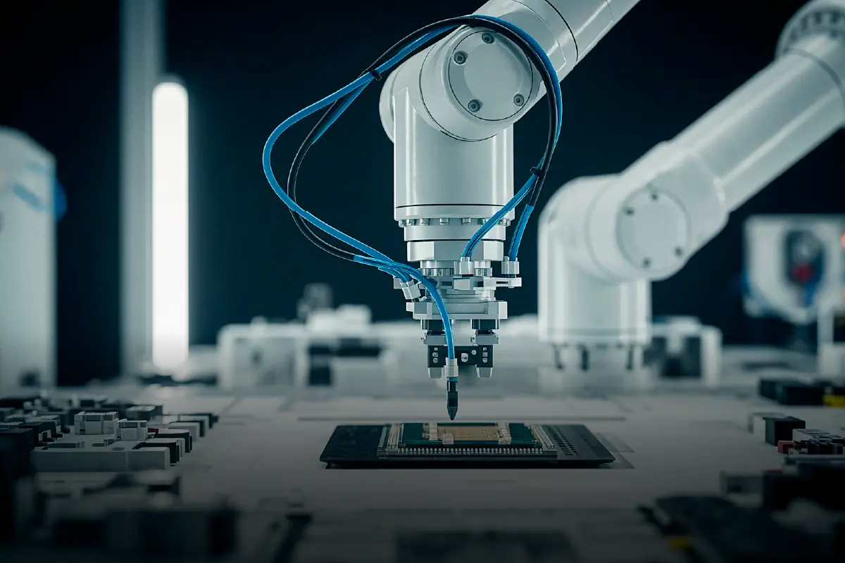
Second, the technology path is not conventional scaling. Sub 2nm requires Gate All Around transistors. GAA replaces the older FinFET structure and wraps the gate around the channel for better control and lower leakage. In simple terms, it squeezes more performance out of less silicon real estate. However, GAA is brutally complex at scale. Yield becomes a battlefield.
Then there is EUV lithography. Extreme Ultraviolet systems are required to pattern features at these dimensions. Without EUV, sub 2nm is theory. With EUV, it becomes capital intensive reality.
But here is where Rapidus is trying to change the rhythm of the industry. It is not chasing only high volume smartphone chips. Instead, it is building what it calls RUMS, Rapid and Unified Manufacturing Service. The focus is fast prototyping, smaller batch production, and rapid iteration cycles for AI startups.
This matters. Because AI companies move faster than legacy chip design cycles. If Rapidus can shorten time from design to silicon validation, it creates a new value proposition. Not scale first. Speed first. That is the wedge.
Geopolitics and Economic Security Driving the Shift
You cannot understand this transition without acknowledging the Taiwan factor.
For decades, global semiconductor manufacturing followed a horizontal model. Design in the United States. Fabrication in Taiwan and Korea. Equipment from Europe. Materials from Japan. It was efficient. It was globalized. It was fragile.
The concept of the Silicon Shield rests on the idea that Taiwan’s semiconductor dominance creates geopolitical deterrence. However, it also concentrates risk. Therefore, countries are recalculating exposure.
Japan is not trying to replace Taiwan. It is trying to reduce systemic vulnerability.
Now look at the capital signals. TSMC, together with Sony Semiconductor Solutions Corporation, DENSO and Toyota, announced further investment into Japan Advanced Semiconductor Manufacturing, Inc. to build a second fab in Kumamoto. It is scheduled to begin operation by the end of 2027. The overall investment exceeds US $20 billion.
That is not symbolic. That is structural.
It tells you that even TSMC sees strategic value in expanding advanced manufacturing presence in Japan. Not because it is trendy. Because diversification is becoming insurance.
At the same time, the World Semiconductor Council brings a broader layer. It is composed of semiconductor associations from Japan, the US, China, Korea, Europe, and Taiwan. It promotes cooperation and issues joint statements supporting open markets and supply chain resilience.
So while national strategies intensify, there is also an effort to keep global coordination alive.
This is the tension. Onshoring without isolation. Sovereignty without fragmentation.
Japan’s move fits inside that balancing act.
Impact on the Global Chip Supply Chain
Now we confront the uncomfortable question. Is this the end of the duopoly?
Today, advanced node leadership sits largely with TSMC and Samsung. Japan entering sub 2nm changes the conversation but not overnight dominance.
The current reality in Japan is anchored by TSMC’s Kumamoto operations. According to its official announcement, the site is intended to produce semiconductors at various process nodes ranging from 40 nm down to 6 and 7 nm.
That range tells you something important. Japan is currently hosting mature to mid-advanced nodes through TSMC’s footprint. Sub 2nm, if achieved by Rapidus, would represent a leap beyond what is presently operational there.
So can Japan challenge the duopoly. Not immediately on volume. However, strategically on capability, yes.
Then comes AI. Sub 2nm is not marketing jargon. AI workloads require higher transistor density and improved power efficiency. Data centers are already under power constraints. Edge computing devices need more performance per watt. Therefore, 2nm becomes a sweet spot for next generation AI accelerators and inference chips.
Moreover, Japan’s materials dominance strengthens the equation. The country controls more than 50 percent of the world’s photoresists and silicon wafers. These are not glamorous products. However, without them, no chip gets built. That upstream leverage matters when scaling advanced nodes.
In other words, Japan already owns critical inputs. Now it is attempting to own advanced logic output.
If Rapidus succeeds, the supply chain shifts from a two pillar structure to three.
However, success depends on execution discipline, not ambition.
The 40,000 Engineer Problem and Other Hard Realities
It is easy to announce fabs. It is hard to staff them.
Japan faces a projected need for 40,000 skilled semiconductor engineers by 2030. That is not a minor hiring campaign. That is workforce reconstruction.
Advanced node manufacturing requires process engineers, equipment specialists, yield analysts, materials scientists, and software integration experts. These skills cannot be produced overnight.
Then comes cost.
Full scale mass production at sub 2nm is projected to require around $35 billion. Funding commitments exist, but scaling to that level introduces budget pressure and potential overruns. Semiconductor fabs are notorious for capital creep. Even small process deviations can inflate cost structures.
Finally, yield.
GAA transistors at 2nm push fabrication physics to extreme limits. Maintaining high yield while introducing new architectures is exceptionally difficult. If yield drops, cost per wafer rises. If cost per wafer rises, competitiveness erodes.
Therefore, the challenge is not just building a fab. It is achieving stable, repeatable, economically viable output.
This is where optimism must meet engineering discipline.
A New Era for Silicon
If Japan executes this transition successfully, it does more than add capacity. It becomes the third pillar of advanced semiconductor manufacturing alongside Taiwan and Korea.
The foundation is already visible. The open R&D center for cutting edge semiconductors in Chitose, Hokkaido is structured as a collaborative hub involving Rapidus and ecosystem stakeholders. It anchors research, manufacturing ambition, and state backing in one location.
By 2027, if timelines hold, the world’s most advanced AI chips could carry a Made in Hokkaido identity. That would signal a structural shift in global supply resilience.
Japan already controls critical materials. Now it is building advanced manufacturing capability. When upstream dominance meets downstream execution, strategic autonomy increases.
The moonshot is real. The risk is real. The global semiconductor map may look very different by the end of this decade.