 日本語
日本語 



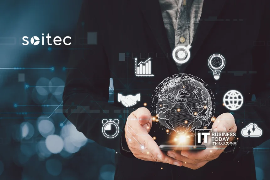
A company that makes materials for semiconductors called Soitec has started offering 500 million euros in convertible bonds. These bonds are called ORNANEs. Will be due in September 2033. The deal is for investors. It is meant to give the company financial freedom as it makes investments in growth and deals with existing debt.
Soitec. Sells advanced materials used in semiconductors. These materials are used in areas like phones, cars, computing at the edge and cloud systems. Its technology that puts silicon on an insulator is also becoming more important for the systems that support intelligence and fast communication.
This funding is happening as the need for semiconductor materials keeps changing along with the growth of AI computing, better connections and advanced electronics.

A Flexible Way to Finance
Each bond will have a value of 100,000 euros. They are expected to have a fixed interest rate between 0.50% and 1.00%. The bonds will be due on September 25 2033. This is unless they are converted, traded paid back or handled in some way before that. Bond owners will also have the right to ask for payment after five years from the day they were issued.
The ORNANE structure gives Soitec choices when the bonds are changed into shares or traded. Depending on the situation payment can be in cash and/or new or existing shares of Soitec. The company has said this way of handling things can help prevent much dilution for current owners because it keeps control over how the payment is made.
Soitec plans to use the money it gets after all the costs, for business purposes. This includes possibly paying off debt and supporting investments that help the company grow.
Financing the Next Semiconductor Cycle
The funding is notable because semiconductor manufacturing is entering a period of increasingly complex demand.
AI data centers require large quantities of advanced computing hardware, while telecommunications, automotive systems and edge devices continue to require specialized semiconductor technologies. This creates demand not only for processors but also for the materials, wafers and manufacturing technologies that enable them.
Soitec’s portfolio includes several silicon-based technologies designed for different applications. Its Photonics-SOI technology is particularly relevant to optical communications, where high-speed data transmission is becoming increasingly important as AI data centers expand.
The company’s September 2026 financing therefore arrives against a backdrop in which semiconductor infrastructure is increasingly being treated as a strategic technology sector.
Photonics Becomes More Important for AI Infrastructure
One area attracting attention is photonics. Traditional electrical connections can face limitations as data volumes increase inside and between computing systems. Optical technologies can help address bandwidth and energy-efficiency requirements in high-speed communications.
Soitec’s management said following the successful bond placement that demand for its Photonics-SOI solutions is accelerating and that the financing would provide additional flexibility to support growth and refinancing.
The development is relevant to the wider AI infrastructure market because the growth of AI workloads is putting pressure on networking systems as well as computing processors. As data centers scale, technologies that improve the movement of information between computing components can become increasingly important alongside advances in processors and memory.
Implications for Japan’s Semiconductor Industry
Soitec’s financing also has relevance for Japan, which is expanding investment across semiconductor manufacturing, materials and advanced packaging.
Japan has a large ecosystem of semiconductor-materials and equipment companies. The country’s strengths include silicon wafers, specialty chemicals, manufacturing equipment and precision technologies. As AI increases demand for advanced chips, these upstream technologies become increasingly important.
The Soitec transaction highlights the capital requirements involved in expanding semiconductor infrastructure. Companies developing advanced materials and manufacturing technologies may need significant funding before new production capacity generates returns.
For Japanese semiconductor companies, the development also reinforces the importance of technologies surrounding AI processors rather than focusing exclusively on the processors themselves. Advanced packaging, optical interconnects, power management and specialized materials are all becoming important components of the broader AI hardware ecosystem.
Competition Moves Beyond Chip Design
The semiconductor industry’s competitive landscape is increasingly extending beyond chip architecture.
Materials companies can influence performance, power consumption, manufacturing yields and the ability to scale new semiconductor technologies. This means developments in materials science can have consequences across data centers, smartphones, vehicles and industrial systems.
For Japan, this creates an opportunity to strengthen its position in parts of the semiconductor value chain where specialized manufacturing expertise and long-term research capabilities are important.
The country is already supporting domestic semiconductor production while encouraging cooperation between international chipmakers and Japanese materials and equipment suppliers. Growing demand for AI infrastructure could further increase the value of these relationships.
Capital and Technology Moving Together
Also Read: Philadelphia Airport Expands Digital Signage for Smarter Passenger Communication
Soitec’s €500 million financing illustrates how financial markets and semiconductor technology development are becoming closely connected.
The company is using a structured financing instrument to maintain flexibility while supporting growth in a sector requiring sustained investment. At the same time, demand for semiconductor materials is being shaped by larger technology trends including AI, optical communications, automotive electronics and cloud computing.
For Japan’s semiconductor ecosystem, the development offers another indication that the next phase of chip investment will extend well beyond fabrication plants. Materials, photonics, packaging and manufacturing technologies will all play roles in determining how quickly the industry can scale to meet demand from AI and other advanced computing applications.


 English