


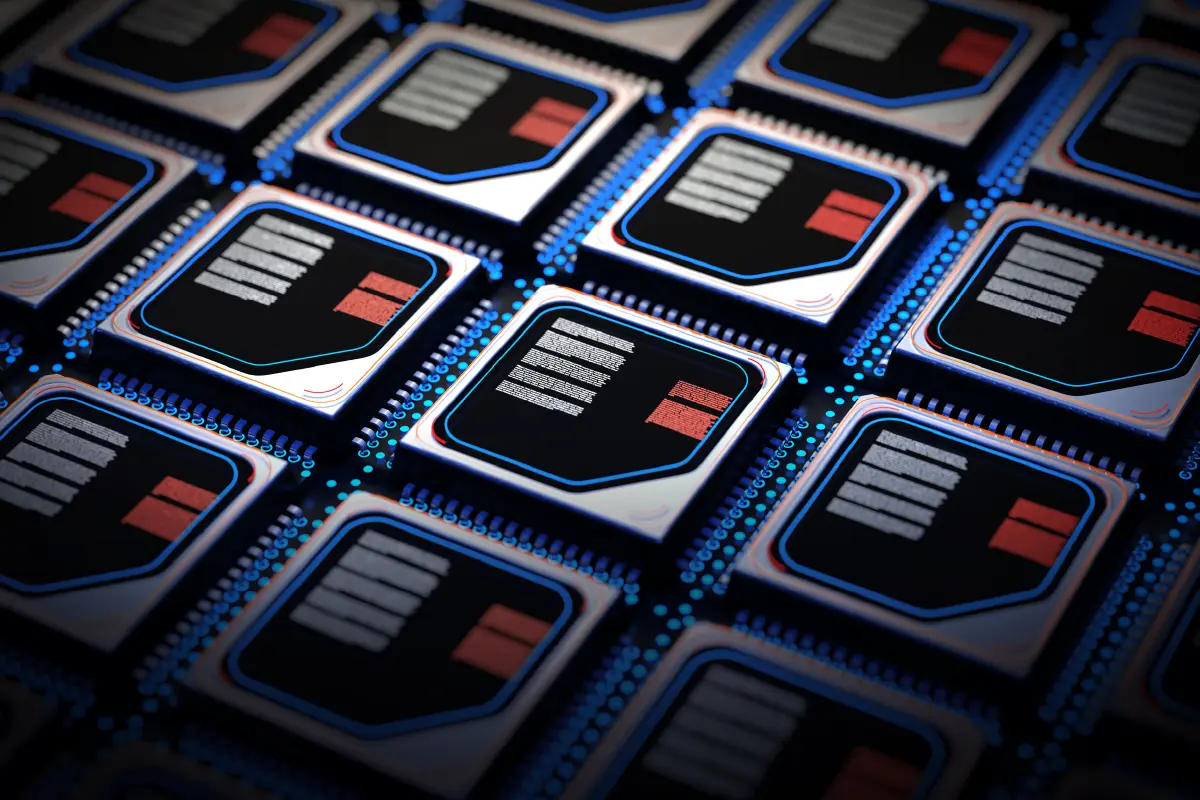
While most headlines obsess over lithography breakthroughs and foundry wars between TSMC and Intel, the real performance battle in AI hardware is happening somewhere quieter. It is happening inside the package. Advanced packaging has become the hidden lever that determines speed, power efficiency, and scalability of modern chips. In this layer of the stack, Japan is not a participant. It is the anchor.
Advanced packaging, in simple terms, refers to the set of technologies that connect multiple semiconductor dies into a single high performance system using techniques like chiplets, 2.5D and 3D stacking, redistribution layers, and through silicon vias. This is where Japan’s materials science and precision manufacturing quietly dominate. The country controls the back end of the front end, supplying the substrates, resins, films, tools, and testing systems that make modern AI chips possible. This is the Japan advanced packaging semiconductor story that most rankings still fail to explain.
Why Packaging Is Becoming the New Moore’s Law
For decades, the semiconductor industry relied on shrinking transistors to deliver performance gains. That model is breaking down. Power leakage, heat, and cost have made monolithic scaling harder with every node. As a result, the industry has shifted toward chiplets and heterogeneous integration, where performance gains come from smarter assembly rather than smaller transistors.

Also Read: The Rise of Ambient Healthcare: When Monitoring Happens Without Interaction
This shift is happening at scale. According to Gartner, global semiconductor revenue reached 793 billion dollars in 2025, growing 21 percent year over year, with AI chip demand acting as the main driver. That growth is not being absorbed by front end manufacturing alone. It is being pulled forward by advanced packaging that allows AI accelerators, memory, and logic to work as one system.
Japan fits into this transition almost naturally. Its long history in chemistry, polymers, ceramics, and ultra-precision engineering maps directly to the needs of advanced packaging. While foundries focus on logic, Japanese suppliers focus on what connects that logic to memory, power, and the outside world. That is why global leaders keep returning to Japan when performance targets rise.
The Eight Japanese Companies Quietly Defining Advanced Packaging
The Japan advanced packaging semiconductor ecosystem is not built around one champion. It is built around a network of specialists, each controlling a critical layer of the stack.
Ibiden sits at the heart of AI server infrastructure. Its IC substrates are designed to handle extreme wiring density and power delivery, which makes them foundational for AI accelerators used in data centers. Without substrates that can support high bandwidth and thermal stability, GPU performance simply stalls.
Shinko Electric Industries pushes the limits of flip chip BGA technology while preparing for the transition toward glass substrates. These substrates promise lower warpage and better signal integrity, both essential as packages grow larger and more complex.
Resonac, formerly Hitachi Chemical, dominates non-conductive films used in high bandwidth memory stacks. As HBM layers increase, the reliability of bonding materials becomes non-negotiable. Resonac’s materials ensure mechanical stability without interfering with electrical performance.
Ajinomoto plays an unusual but critical role through Ajinomoto Build up Film. ABF acts like the ingredient brand of the chip world. It enables ultra-fine wiring in substrates used by high end CPUs and AI processors. Without it, modern package densities would not be possible.
DISCO Corporation enables the physical reality of 3D stacking. Its dicing and grinding tools allow wafers to be thinned precisely without damage, which is essential for stacking memory and logic vertically.
Tokyo Electron focuses on the processes that bond wafers together. Wafer on wafer techniques and hybrid bonding sit at the core of next generation 3D integration, and TEL’s tools enable consistent yields at scale.
Advantest ensures that complex multi die packages actually work before they ship. As packages grow more intricate, testing becomes as critical as manufacturing itself.
Namics supplies advanced adhesives and underfills that manage stress, heat, and long term reliability inside dense packages.
Each of these companies owns a narrow but essential slice of the advanced packaging stack. Together, they form a system that competitors struggle to replicate.
How CoWoS and HBM Depend on Japanese Materials
One of the clearest examples of Japan’s influence is TSMC’s CoWoS technology, which stands for chip on wafer on substrate. CoWoS enables high performance GPUs by placing logic and memory close together with massive bandwidth. The substrates, resins, and bonding materials that make this possible largely come from Japan.
High bandwidth memory is evolving rapidly, moving toward HBM3e and HBM4 with taller stacks and tighter tolerances. As stacks grow, the margin for material failure disappears. Japanese films and resins provide the mechanical stability and thermal control required at these extremes.
At the high end of the market, Japan effectively controls the supply of ABF used in advanced substrates. This makes it a structural chokepoint in the global supply chain. Performance roadmaps depend on materials that cannot be easily substituted or scaled elsewhere.
Power Efficiency and Sustainability Inside the Package
Advanced packaging is not just about speed. It is also about power. By shortening interconnects and enabling vertical integration, 3D packaging reduces energy lost during data movement. Industry discussions led by SEMI consistently highlight chiplets and 3D integration as central to improving power efficiency and thermal performance.
Japanese material innovation plays a direct role here. Better thermal interfaces, lower resistance interconnects, and more stable bonding materials reduce leakage and heat buildup. In a world where data centers strain power grids, these gains matter as much as raw performance.
Geopolitics, Rapidus, and the Back End Bet

Japan’s government understands that its strategic advantage lies in the back end as much as the front end. Through initiatives tied to Rapidus, the country is aligning advanced logic ambitions with packaging and materials strength. According to the Ministry of Economy, Trade and Industry, Japan committed 1.85 trillion yen to semiconductor support in 2023, with further increases planned through fiscal year 2026. A meaningful portion of this effort targets ecosystem resilience rather than just node leadership.
This approach reflects a long term view. Control the materials and packaging, and you influence every foundry and every AI roadmap that depends on them.
The Road to 2030 and Why Japan Matters
The next era of semiconductors will not be defined by transistors alone. It will be defined by how chips are assembled, connected, and powered. Advanced packaging sits at the center of that shift.
For engineers, Japan represents reliability at scale. For investors, it represents defensible chokepoints. For policymakers, it represents leverage without confrontation. The Japan advanced packaging semiconductor ecosystem does not chase headlines. It shapes outcomes. As AI hardware grows more complex, the quiet strength of Japanese materials and packaging will only become harder to ignore.